Нет товаров
Товар добавлен в корзину
Товаров в корзине: 0. Сейчас в корзине 1 товар.
N4880A
N4880A

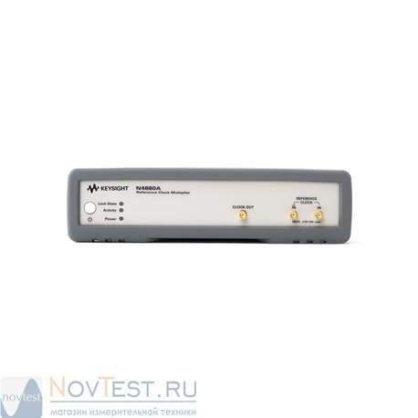
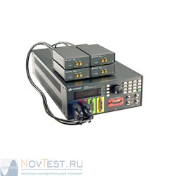
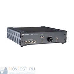
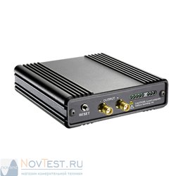
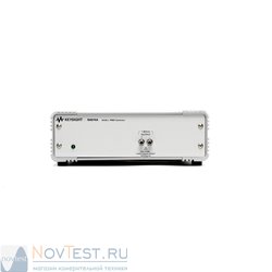
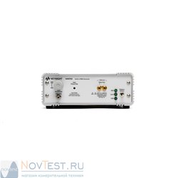
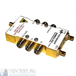
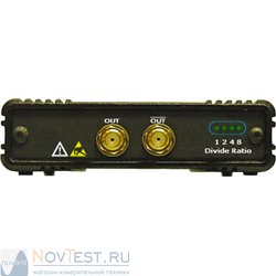
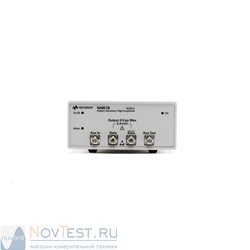
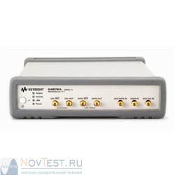
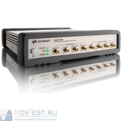
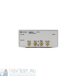
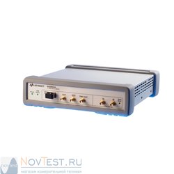
N4880A Reference Clock Multiplier
- Убрать этот товар из моего избранного.
- Добавить этот товар в избранное.
- Печать
Описание - N4880A
Загрузить техническое описание
Accurate and simplified receiver testing for PCI Express, MIPI M-PHY and SD UHS-II
The N4880A reference clock multiplier fills a critical requirement for R&D and test engineers who need to characterize and release the next generation of PCI Express main boards, MIPI M-PHY chipsets and SD card UHS-II host devices. With its support for multiple reference-clock rates, the N4880A will help you accurately characterize and verify standards compliance under easy-to-reproduce test conditions.
Lock the stressed-pattern generator to a system reference clock
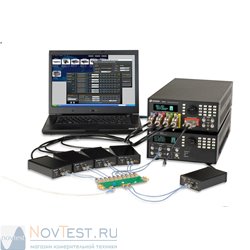
In common reference-clock architectures, where the host cannot be driven by an external reference clock it’s necessary to lock the stressed-pattern generator to the same system reference clock used by the receiver under test. This is because the receiver under test also derives its sampling clock from this reference clock. Locking the stressed pattern generator to the same reference clock as the receiver under test ensures accurate and reproducible jitter-tolerance test results.
Get the most precise and reproducible receiver tolerance test results for PCI Express mainboards, MIPI M-PHY and SD UHS-II hosts
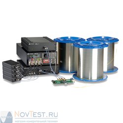
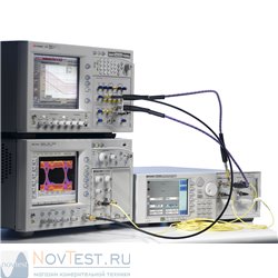
The N4880A provides a multiplying phase-locked loop (PLL) which enables users to lock the pattern generator of J-BERT N4903B or ParBERT 81250A to a system reference clock. Spread Spectrum Clocking (SSC) and low frequency jitter are fed through the N4880A up to its PLL loop bandwidth of 2 or 5 MHz. The N4880A tolerates huge amounts of SSC for UHS-II reference clocks and offers excellent input sensitivity to handle very low voltage levels.
Increase your R&D efficiency with a future-proof investment
By using N4880A for receiver test, R&D engineer’s efficiency is increased as the test complexity is reduced by eliminating complicated and time-consuming work-arounds. The R&D investment is secured by usage for multiple emerging standards.
PCI-SIG®, PCIe® and the PCI Express® are US registered trademarks and/or service marks of PCI-SIG.
MIPI is a licensed trademark of MIPI, Inc. in the U.S. and other jurisdictions.
- Supports accurate and repeatable receiver testing for PCI Express® 1.0,2.0, 3.0, MIPI™ M-PHY gear 1-3 and SD card UHS-II
- Multiplies 19.2 MHz, 26 to 52 MHz, 100 MHz reference clocks to an external clock signal for J-BERT N4903B or ParBERT 81250A pattern generators
- Remains transparent to 33 kHz SSC on reference clock through multiplying PLL (2 or 5 MHz loop bandwidth)
- Tolerates small input signals with input sensitivity of 100 mVpp differential
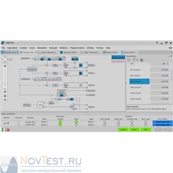
- Enables easy operation and remote control through USB connection and standalone graphical user interface


